Apr 09, 2025·8 min
GlobalFoundries: Specialty Nodes and a Multi-Region Strategy
Learn how GlobalFoundries stays competitive without chasing the smallest nodes—using specialty processes and a multi-region manufacturing footprint.
Why foundries can win without the smallest nodes
“Bleeding edge” in semiconductors usually means the newest process nodes with the smallest transistors. Smaller transistors can boost performance and lower power, but they also require extreme equipment, huge R&D budgets, and long development cycles. The result is straightforward: the very latest nodes are the most expensive to build, the hardest to ramp, and the most constrained when demand spikes.
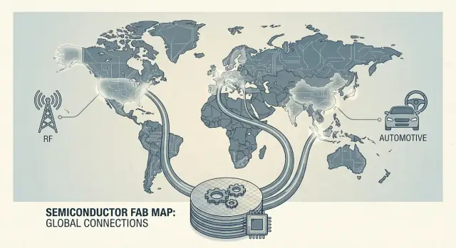
GlobalFoundries’ relevance comes from a different playbook: specialization and location. Instead of chasing the absolute smallest geometry, it focuses on specialty process nodes and manufacturing in multiple regions—two levers that can matter as much as transistor size for many real products.
Specialization beats shrink for many chips
A lot of chips don’t need the tiniest transistors; they need the right features. Think about built-in capabilities like RF performance for phone connectivity, high-voltage tolerance for automotive power systems, or long-term reliability for industrial controls. These requirements often map better to proven, mature nodes that have been tuned for specific use cases.
Location reduces supply risk
Where a chip is made has become a strategic choice, not just a cost decision. Regional manufacturing can help customers manage shipping uncertainty, export controls, and qualification needs—especially for regulated or safety-critical markets.
Who benefits from this approach
This strategy tends to fit organizations shipping products with long lifetimes and strict reliability requirements, including automotive, mobile RF, industrial and IoT systems, and aerospace/defense programs.
This article is a strategy overview—how specialty nodes and a multi-region footprint can keep a foundry competitive—not a financial report or a node-by-node scorecard.
Specialty nodes: what they are and why they matter
“Specialty nodes” are semiconductor manufacturing processes built to optimize specific capabilities—like radio performance, power efficiency, high-voltage tolerance, or embedded non-volatile memory—rather than chasing the smallest possible transistor dimensions.
By contrast, leading-edge logic focuses on the newest, smallest nodes (often used for top-end CPUs/GPUs and some smartphone processors) where the main goal is pushing peak compute performance per watt through aggressive scaling.
Why many products don’t need the newest node
A huge share of chips aren’t bottlenecked by raw transistor density. They’re limited by analog behavior, operating voltage, temperature range, certification needs, or simply the economics of the end product.
For these devices, moving to a leading-edge node can raise costs without delivering meaningful value. Mask sets and design effort are more expensive, manufacturing can be more complex, and qualification cycles can take longer. Many markets—especially automotive, industrial, and infrastructure—also demand long lifetimes and stable supply. A process that stays available for years (sometimes a decade or more) is often more important than squeezing out the last bit of density.
Common terms you’ll hear
Mature nodes generally mean well-established process generations that have been in high-volume production for a while (often 28nm and above, though the exact cutoff varies). Mature doesn’t mean “obsolete”—it often means predictable yields, proven reliability, and a deep ecosystem of qualified IP.
Feature size is the physical dimensions of structures on the chip, but modern processes have many critical dimensions, so it’s not a single number.
A process platform is the broader “recipe” and toolset behind a node—such as an RF-optimized platform, a high-voltage platform, or an embedded-memory platform. Two foundries might both offer “22nm,” yet the platforms can be tuned for very different outcomes.
A note on node names
Node labels aren’t perfectly comparable across foundries. “14nm” or “28nm” can describe different transistor designs, metal stacks, and density targets depending on the manufacturer. That’s why customers evaluate real metrics—power, performance, RF behavior, voltage options, reliability data, and total cost—not the node name alone.
Where demand stays strong: long-life and high-reliability chips
A large share of the semiconductor market isn’t chasing the newest node. Many buyers prioritize chips that keep shipping for a decade (or longer), behave the same from lot to lot, and are backed by a tightly controlled manufacturing process.
What these customers actually need
For long-lifecycle products, the “spec” is more than performance and cost. Typical requirements include:
- Long availability windows: the same part (or a qualified equivalent) must remain purchasable for years, often aligned to the life of a vehicle platform or industrial system.
- Stable yields and predictable output: manufacturers want consistent wafer starts, predictable delivery schedules, and fewer surprises as volumes ramp or fluctuate.
- Qualification and reliability evidence: automotive and industrial buyers may require extensive testing, documented process controls, and ongoing monitoring.
- Strict change control: even small process changes can trigger re-qualification, so customers value continuity over frequent tweaks.
Why “just move to a newer node” is rarely simple
Redesigning to a newer process node can be expensive and risky, especially when the chip is one component inside a larger certified system. Porting a design may involve new IP, new packaging, updated verification, additional reliability testing, and software validation. The engineering effort can be significant—and the business impact of a schedule slip (or a post-launch field issue) can far outweigh any theoretical cost or performance benefit.
Lifecycle-driven markets keep demand steady
Cars, factory equipment, power infrastructure, aerospace, and networking gear are built around service life and uptime. These markets reward foundries that deliver:
- consistent supply across product generations,
- well-understood, repeatable processes,
- and clear policies for revisions, notifications, and continuity.
In other words, demand stays strong where predictability is the product—because reliability and availability are often the real differentiators.
Key specialty technologies GlobalFoundries is known for
GlobalFoundries is best known for process “platforms” that are tuned for specific chip jobs—especially radio-frequency, power, and mixed-signal devices that don’t benefit much from chasing the smallest geometry.
RF SOI for smartphone radios
A flagship example is RF SOI (radio-frequency silicon-on-insulator). In plain terms, RF SOI builds transistors on a thin silicon layer separated from the bulk silicon by an insulating layer. That insulation reduces unwanted electrical leakage and coupling, so high-frequency signals stay cleaner.
For smartphones, that matters because the front-end radio has to switch and filter tiny signals across many bands without wasting battery or creating interference. RF SOI is widely used for RF switches, tuners, and other circuits that sit between the modem and the antenna.
Power management and mixed-signal: voltage handling and analog quality
Phones, cars, and industrial systems still need chips that can handle higher voltages and deliver stable power. Power-management ICs and mixed-signal parts care less about raw digital density and more about:
- Analog performance (low noise, precision)
- High-voltage devices (to move power efficiently)
- Integration (putting analog, power, and some digital control together)
These platforms are often built on mature nodes because they’re proven, cost-effective, and easier to qualify for long product lifetimes.
Embedded NVM and other specialty options
Many products also benefit from embedded non-volatile memory (eNVM)—memory that keeps data when power is off. At a high level, this enables storing calibration data, IDs/keys, and configuration without adding a separate memory chip, which can simplify the bill of materials and improve reliability.
Where these technologies show up
You’ll often find these specialty processes inside end products like:
- 5G front-end modules (switching and tuning)
- Wi‑Fi and connectivity components
- Power ICs (battery charging, regulation)
- Sensor hubs and always-on controllers
The common thread: these chips win on RF behavior, power efficiency, and reliability—not on being the smallest transistor available.
Performance beyond scaling: how products improve without shrink
Model regional supply risk
Create a multi-region continuity tracker for sites, constraints, and contingency actions.
It’s easy to assume progress in semiconductors means “more transistors on a smaller node.” But many real-world products improve because the whole system gets better: lower power draw, less electrical noise, less heat, and more predictable behavior over time. For customers building cars, factory equipment, networks, and phones, those system-level gains often matter more than a raw transistor count.
“Better” can mean cooler, quieter, and more efficient
Shrinking can help performance, but it also raises design complexity and cost. On specialty and mature nodes, engineers can still hit modern targets by optimizing what the chip does and how it interacts with the rest of the product:
- Power: smarter power management and mixed-signal blocks that waste less energy
- Noise: cleaner analog/RF behavior for stable wireless and sensing
- Heat: more efficient operation and packaging that spreads heat effectively
Packaging and co-design (in plain English)
Think of packaging as how chips are assembled into a usable part. Instead of one giant “do-everything” chip, companies increasingly combine multiple dies into a single package:
- Chiplets: smaller chips that each handle one job (compute, I/O, RF, power)
- Modules: a packaged “mini-system” that can include multiple chips plus filters, passives, and shielding
With co-design, the chip and package are planned together so the whole unit meets performance goals—like reducing interference, shortening signal paths, or improving heat dissipation.
Older nodes + smart packaging can meet modern requirements
A simple example is a smartphone:
- The application processor chases leading-edge nodes to maximize compute per watt.
- The RF front-end module (amplifiers, switches, tuning, filtering) often benefits more from specialty processes and module integration, where low noise and consistent RF characteristics are crucial.
This is where foundries like GlobalFoundries stay relevant: by enabling “better system performance” without forcing every component onto the smallest node. For more on where this matters most, see /blog/specialty-nodes-explained.
Geographic strategy: reducing risk through regional manufacturing
A chip’s “where” matters almost as much as its “what.” For customers building products with long lifetimes—automotive modules, industrial controls, networking equipment—supply risk isn’t abstract. Geopolitics can disrupt trade routes, logistics delays can stretch schedules, and single-region concentration can turn a local outage into a global production stop.
What “regional capacity” means in practice
Regional capacity is more than putting a pin on a map. It usually means having meaningful manufacturing volume in multiple regions, supported by local supplier networks and operational know-how. For customers, that can translate into:
- Shorter physical shipping lanes for wafers and packaged parts
- Fewer chokepoints where a single port, border, or carrier issue halts deliveries
- Better alignment with local qualification expectations and customer audit needs
Just as importantly, it offers optionality: if demand shifts or a disruption hits one area, customers may have a pathway—sometimes over time and with re-qualification—to keep critical products flowing.
Risk management: lead times, logistics, and continuity
Semiconductor lead times include more than fab cycle time. Mask delivery, specialty gases, photoresists, substrates, assembly/test capacity, and cross-border customs can all become constraints. A multi-region approach aims to reduce the chance that one constraint cascades through the whole chain.
This doesn’t eliminate risk; it spreads it. Customers still need to plan buffers, dual-source where feasible, and understand the qualification effort required to move a product between sites.
The trade-offs foundries and customers live with
Regional manufacturing isn’t automatically cheaper or faster. New capacity can involve higher labor costs, tight talent markets, and long timelines for utilities hookups and permitting. Energy pricing, water availability, and local infrastructure can also affect operating cost and schedule reliability.
For many buyers, the decision becomes a balancing act: accept some added cost or complexity in exchange for improved continuity and a supply chain that’s less dependent on any single region.
What customers look for: resilience, qualification, and continuity
For many chip buyers, the deciding factor isn’t the newest node—it’s confidence that parts will keep shipping, unchanged, for years. That’s why conversations with foundries often start with resilience and continuity rather than transistor counts.
Resilience: more than “can you make it?”
Customers increasingly ask about second sources and “what if” scenarios. Sometimes that means a true dual-sourcing plan (two qualified foundries). Other times it’s a dual-region option within the same foundry: the same process platform available in more than one fab region, with a realistic path to move volume if one site is constrained.
Even when dual-region manufacturing is possible, buyers want specifics: expected transfer timelines, what data must be re-run, and how much of the toolset and materials are matched across sites.
Qualification and documentation (especially automotive)
In automotive and other safety- or mission-critical markets, qualification is a project of its own. It’s not just “the chip works,” but “the process is controlled.” Customers expect disciplined documentation—process change notifications, traceability, reliability test data, and clear rules for lot acceptance.
They may also require long-term stability commitments: frozen design rules, controlled mask changes, and strict limits on material or equipment substitutions. These requirements can add time up front, but they reduce surprises later.
Continuity planning: business continuity you can audit
A credible continuity plan covers capacity reservation, supply assurance for key materials, and a playbook for surge demand. A multi-site footprint can support this by offering alternate capacity, different local utilities, and separation from single points of failure.
Diversification doesn’t eliminate risk—it reshapes it. Multiple regions can lower exposure to a local outage, but introduce new dependencies (logistics, export controls, regional suppliers). Customers tend to favor foundries that can explain those trade-offs clearly and show how they’re monitored over time.
The business model: platform depth over node races
Bring your team onboard
Invite teammates or partners and get referral credits as your tooling expands.
Specialty-focused foundries compete differently from the companies chasing the smallest geometry. Leading-edge nodes demand massive up-front spending: years of R&D, new toolsets, and frequent process rework as designs push physics limits. That model only pays off if you can keep very expensive capacity full with high-volume, short-cycle products.
By contrast, a specialty-node business tends to emphasize platform depth—a process family that stays in production for a long time, accumulates options, and gets reused across many customers and chip types. The goal is less about “the newest node” and more about a factory running efficiently: high utilization, steady yields, and predictable schedules.
Why stability becomes a product
A stable process is valuable because it reduces re-qualification and redesign. Once a platform has proven reliability, customers can reuse building blocks—design rules, IP, packaging choices, test programs—across multiple product generations. That reuse shortens development time and lowers risk, even when the transistor size doesn’t change.
Foundries also benefit: each additional product that fits the same platform spreads process-development effort across a wider base, making incremental improvements (yield, reliability, optional modules) more worthwhile.
What drives pricing (in plain terms)
Pricing in foundry work usually follows practical constraints rather than hype:
- Tool availability: If a specific tool type is scarce or booked out, that step becomes a bottleneck and adds cost.
- Yield and maturity: A well-understood process with high yield wastes fewer wafers, which supports more consistent pricing.
- Volume and mix: Large, predictable runs are easier to plan. Highly variable demand or many small runs can raise per-unit cost.
This is why platform businesses invest heavily in repeatable “recipes” and long-lived capacity planning instead of constant node races.
Use-case snapshots: automotive, mobile RF, and industrial
Specialty nodes show their value when you look at how products are actually built, qualified, and supported over time. Below are three common patterns where a foundry like GlobalFoundries can be a fit—without implying any specific customer contract or program.
Automotive: reliability and long commitments
Automotive silicon is often selected as much for its “will it still ship in 10–15 years?” profile as for raw performance. Designs may need extended temperature operation, conservative voltage margins, and detailed qualification flows that take time.
A typical example is a controller or interface chip that must keep the same electrical behavior across multiple vehicle generations. In these cases, mature and specialty process options can reduce re-validation risk, while long product support policies and stable manufacturing change control become central buying criteria.
Mobile / RF: volume, cycles, and integration
RF front-end and connectivity parts live in a world of high volumes and frequent refreshes. Here, “better” isn’t always “smaller node”—it can be lower loss, better matching, tighter integration of RF switches with control logic, or improved power handling.
An illustrative scenario is a handset-related RF module where fast product cycles demand predictable ramp capacity and repeatable RF performance. Specialty RF process technologies can help teams hit targets for efficiency and signal integrity while keeping cost and yield in check.
Industrial / IoT: diversity and cost discipline
Industrial and IoT portfolios often span many SKUs, with uneven demand and long field lifetimes. Cost sensitivity is high, but so is the need for consistent availability—especially for sensors, motor control, power management companions, and connectivity.
A practical example is an industrial gateway platform: it may combine multiple mature-node chips (MCU, interfaces, analog, security) where continuity, second-source planning, and packaging/test options matter as much as transistor density.
If you’re collecting real-world examples for your own evaluation, focus on requirements (temperature, qualification standard, lifetime supply, RF specs, packaging) rather than naming customers—those constraints tell you far more about foundry fit.
How GlobalFoundries fits among other foundry options
Keep ownership of your code
Build the tool fast, then export source code when your team wants full control.
Choosing a foundry isn’t a simple “best vs. rest” decision. Most customers are really choosing a fit—for performance needs, risk tolerance, volume ramp, and how long a product must stay in production.
The main competitor categories
Leading-edge giants focus on the newest nodes and extreme transistor density for flagship CPUs, GPUs, and top-tier mobile SoCs. Think of players like TSMC and Samsung, and (in a different model) Intel Foundry. Their advantage is cutting-edge scaling and ecosystem gravity around advanced packaging and the latest design flows.
Mature-node and specialty-focused foundries prioritize proven nodes, analog/RF capabilities, embedded non-volatile memory options, and longer product lifetimes. This group includes companies such as UMC, SMIC, Tower Semiconductor, and others—often with deep expertise in specific device types rather than a race to the smallest geometry.
Where GlobalFoundries differentiates
GlobalFoundries generally competes on three levers:
- Specialty process portfolio: strong offerings where “better” means lower power, higher RF performance, or better isolation—not just smaller transistors (for example, RF-focused processes and other differentiated platforms).
- Manufacturing footprint: a multi-region approach can be attractive for customers managing compliance, trade exposure, or continuity requirements.
- Customer support and operational maturity: predictable qualifications, stable design kits, and a focus on repeatable high-yield manufacturing for long-lived products.
Switching costs are real
Moving a design between foundries can be expensive even when nodes look similar on paper. Common friction points include different design rules/PDKs, availability of qualified IP (I/O, PLLs, memory compilers), and time-consuming requalification for automotive, industrial, or medical use. Add in mask costs, yield learning, and reliability testing, and “just port it” often becomes a multi-quarter effort.
If you want a quick refresher on why specialty nodes matter in the first place, see /blog/specialty-nodes.
Choosing a foundry path: practical questions and next steps
Selecting a foundry isn’t only about “how small can you go.” It’s about matching your product’s real needs—performance, reliability, cost, and supply continuity—to a manufacturing platform you can live with for years.
A quick decision flow
Start simple:
- Do you truly need leading-edge nodes? If your product depends on maximum compute density (flagship CPUs/GPUs/AI accelerators), you may.
- If not, what specialty capability is the differentiator? Common drivers include RF performance, high-voltage/power, embedded non-volatile memory, low-leakage, or automotive-grade reliability.
- Then choose the geography and continuity plan that reduces your supply risk (single-site vs. multi-region options).
Checklist: what to align before you commit
Use this as a practical pre-RFQ checklist:
- Node needs: performance target, power budget, die size limits, cost target
- Specialty features: RF front-end support, high-voltage devices, eNVM, analog/mixed-signal needs
- Supply geography: preferred regions, export-control considerations, second-source expectations
- Qualification: automotive/industrial requirements, reliability targets, audit expectations
- Packaging/test: required packages, OSAT preferences, known-good-die needs, yield learning plan
- Volume & ramp: forecast ranges, surge capacity, lifecycle expectations (5–15+ years)
Questions to ask a foundry partner
Ask for specifics early:
- What are typical lead times for wafers, masks, and packaging?
- How stable is the process roadmap for this platform over the next 3–5 years?
- What is the change-control policy (PCNs, notice periods, qualification of changes)?
- How do you handle capacity allocation during shortages?
- What are the options for multi-site manufacturing or contingency plans?
If you want help turning these answers into a shortlist and timeline, see /pricing or reach out via /contact.
Practical note for ops and engineering teams: once you’ve chosen a foundry strategy, the next bottleneck is often execution—tracking RFQs, qualification evidence, multi-site options, and change-control decisions across teams. Platforms like Koder.ai can help you stand up internal tooling (dashboards, approval workflows, supplier and part tracking, audit-ready documentation portals) quickly by building web apps via chat, with source-code export and rollback support. For organizations operating across regions, that speed-to-tooling can be a meaningful complement to the “resilience and continuity” mindset described above.