May 02, 2025·8 min
KLA and Fab Yield: Inspection & Metrology That Cut Cost
A practical guide to how KLA-style inspection and metrology shape yield, scrap, cycle time, and cost—plus what to track and how fabs choose tools.
A practical guide to how KLA-style inspection and metrology shape yield, scrap, cycle time, and cost—plus what to track and how fabs choose tools.
Inspection and metrology are the fab’s “eyes,” but they look for different things.
Inspection answers: Is something wrong somewhere on the wafer? It scans for defects like particles, scratches, pattern breaks, contamination, or subtle anomalies that correlate with future failures.
Metrology answers: Is the process doing what we intended? It measures critical dimensions (CD), overlay (layer-to-layer alignment), film thickness, and other parameters that determine whether the chip will function.
A fab can only control what it can measure—yet measurement itself consumes tool time, engineering attention, and queue space. That creates a constant trade-off:
If inspection is too slow, defects can spread across lots before anyone notices. If metrology is too noisy, engineers may “chase ghosts,” adjusting a process that wasn’t actually drifting.
Most of the highest-impact fab decisions aren’t dramatic—they’re routine calls made dozens of times per day based on measurement data:
These calls quietly determine yield, cycle time, and cost per wafer. The best fabs don’t just “measure a lot”—they measure the right things, at the right frequency, with confidence in the signal.
This article focuses on concepts you can use to understand how vendors like KLA fit into yield management—why certain measurements matter, how they drive action, and how they affect economics.
It won’t dive into proprietary specifications or model-by-model claims. Instead, it will explain the practical logic behind inspection and metrology choices, and how those choices ripple into competitiveness.
A wafer doesn’t “get measured once.” It gets checked repeatedly as it moves through loops of patterning and material change. A simplified path looks like: lithography (print the pattern) → etch (transfer it) → deposition (add films) → CMP (planarize) → repeat for dozens of layers → electrical test and final sort.
Measurements are inserted right where variation becomes expensive to fix later:
Fabs don’t measure everything at the same rate. Critical layers (tight design rules, sensitive overlay budgets, new process steps) tend to get higher sampling—more wafers per lot, more sites per wafer, and more frequent inspection. Less critical or mature layers often use lighter sampling to protect throughput.
The sampling plan is a business decision as much as a technical one: measure too little and escapes rise; measure too much and cycle time suffers.
The practical goal is balance: enough inline coverage to steer the process in time, plus targeted offline work when the data says something has changed.
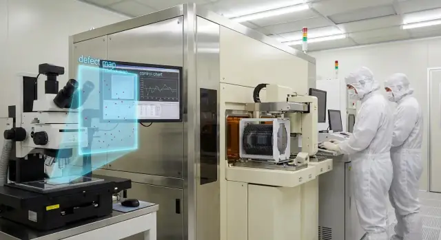
Inspection is often described as “finding defects,” but the operational job is deciding which signals are worth reacting to. A modern fab can generate millions of defect “events” per day; only a fraction affect electrical performance. Platforms and tools (including KLA-class systems) help turn raw images into decisions—but the trade-offs are always there.
Defects vary by layer, pattern, and process step:
Many of these look similar at first glance. A bright “blob” might be a harmless resist speck on one layer, but a yield killer on another.
A killer defect is one that is likely to cause a functional failure (opens, shorts, leakage, parametric shift). A nuisance defect is real or apparent but doesn’t impact yield—think cosmetic pattern roughness that stays within margin.
Classification matters because fabs don’t just pay for detection; they pay for what detection triggers: review time, lot holds, rework, engineering analysis, and tool downtime. Better classification means fewer expensive reactions.
At a high level, defect density is “how many defects per unit area.” As chips get larger or design rules tighten, the probability that at least one killer lands in a critical area rises. That’s why reducing killer defect density—even modestly—can create a noticeable yield lift.
No inspection system is perfect:
The goal isn’t “find everything.” It’s to find the right things early enough—and cheaply enough—to change outcomes.
Metrology is how a fab turns “the tool ran” into “the pattern is actually what we intended.” Three measurements show up everywhere in yield learning because they connect directly to whether transistors and wires will work: critical dimension (CD), overlay, and drift.
CD is the measured width of a printed feature—think of the gate length of a transistor or the width of a narrow metal line. When CD is even slightly off, electrical behavior shifts quickly: too narrow can increase resistance or cause opens; too wide can short to neighbors or change transistor drive current. Modern designs have tiny margins, so a few nanometers of bias can move you from “safe” to “systematic failure” across many dies.
CD problems often have recognizable focus/exposure signatures. If focus is off, lines may look rounded, necked, or “pinched.” If exposure dose is off, features can print too big or too small. These are pattern fidelity issues: the shape may be distorted even if the average width looks acceptable.
Overlay measures how well one layer aligns to the previous layer. If alignment errors accumulate, vias miss their targets, contacts land partially, or edges overlap in the wrong places. A chip can have “perfect” CDs on each layer and still fail because the layers don’t line up.
At a high level, fabs use optical metrology for fast, high-throughput measurements and SEM-based metrology when they need sharper, more detailed views of tiny features. Vendors are chosen based on how well the measurements catch real drift early—before it turns into lot-wide yield loss.
Process drift is the quiet enemy: temperature, chemistry, tool wear, or reticle changes can nudge CD and overlay slowly, until the fab is suddenly outside spec.
Measurements only reduce cost when they trigger consistent decisions. That “last mile” is Statistical Process Control (SPC): the routine that turns inspection and metrology signals into actions operators trust.
Imagine a CD measurement after an etch step starts drifting wider.
Feedback control is the classic loop: you measure the result, then adjust the etcher recipe so the next lot lands back on target. It’s powerful, but it’s always a step behind.
Feedforward control uses upstream information to prevent the error from showing up later. For example, if lithography overlay or focus measurements indicate a known bias on a specific scanner, you can automatically adjust downstream etch or deposition settings before processing the lot.
SPC charts draw control limits (often based on process variation) around a target. When data crosses those limits, it’s an excursion—a sign the process changed, not just normal noise.
If teams routinely override alarms because “it’s probably fine,” two things happen:
Trusted alarms enable fast, repeatable containment: stop the line for the right reasons, not constantly.
Latency is the time between processing and a usable measurement. If CD results arrive after multiple lots are already run, feedback corrections fix the future while defects pile up in the present. Lower latency (or smarter sampling) shrinks the “at-risk” material and improves both feedback and feedforward.
When limits, response plans, and ownership are clear, fewer lots go on hold “just in case,” and fewer wafers need expensive rework. The payoff is quieter operations: less variability, fewer surprises, and faster yield learning.
Measurement isn’t “overhead” in a fab—it’s a set of choices that either prevents expensive mistakes or creates expensive busywork. The cost impact shows up in predictable buckets:
Higher sensitivity in inspection (for example, pushing to smaller defect sizes) can reduce escapes—but it can also flood engineering with nuisance signals. If every “possible defect” becomes a hold, the fab pays in tool idle time, queue growth, and analysis labor.
The economic question is not “Can the tool see it?” but “Does acting on it prevent more loss than it creates?”
Where you measure more—or less—matters as much as which tool you buy. High-risk layers (new process steps, tight overlay layers, known excursion points) usually deserve denser sampling. Stable, mature layers may be better served by lighter sampling plus strong SPC guardrails.
Many fabs use inspection/metrology outputs to tune this layer-by-layer: increase coverage where excursions are frequent, and pull back where signals rarely drive action.
A good catch: early detection of a focus drift that would have degraded an entire lot, enabling a quick correction and saving downstream litho/etch steps.
Expensive noise: repeatedly flagging benign patterning artifacts that trigger holds and reviews, while yield and electrical results stay unchanged—burning cycle time without reducing scrap.
Yield learning doesn’t happen “for free.” Every inspection scan, metrology sample, and defect review consumes scarce tool time—and when that capacity is tight, measurement becomes a factory constraint that stretches cycle time.
Most cycle-time impact isn’t the scan itself; it’s the waiting. Fabs commonly see queues build at:
Those queues slow lots across the line, increase WIP, and can force suboptimal decisions—like skipping confirmatory measurements just to keep material moving.
Planning measurement capacity isn’t just “buy enough tools.” It’s matching capacity to recipe mix. A long, sensitive inspection recipe can consume multiples of the tool time of a lightweight monitor.
Key levers fabs use:
Automation improves cycle time when it reduces the “in-between” work:
The biggest payoff of speed is learning. When inspection and metrology results flow quickly into a clear, actionable diagnosis, the fab avoids repeating the same excursion across multiple lots. That reduces rework, scrap risk, and the compounding cycle-time hit of “more sampling because we’re worried.”
Shrinking features doesn’t just make chips faster—it makes measurement harder. At advanced nodes, the “allowable error” window gets so small that inspection sensitivity and metrology precision must improve at the same time. The consequence is simple: a defect or a few nanometers of drift that was harmless before can suddenly flip a wafer from “good” to “marginal.”
EUV changes the defect and metrology problem in a few important ways:
This pushes fabs toward more sensitive inspection, smarter sampling, and tighter links between what’s measured and what’s adjusted.
Even with EUV, many layers involve multi-patterning steps and complex 3D stacks (more films, more interfaces, more topography). That raises the chance of:
Metrology targets can become less representative, and recipes often need frequent tuning to stay correlated to yield.
Not every layer needs the same sensitivity or precision. Logic, memory, and power devices emphasize different failure mechanisms, and within one chip, gate, contact, via, and metal layers can demand very different inspection thresholds and metrology uncertainty. Winning fabs treat measurement strategy as layer-by-layer engineering, not a one-size setting.
Inspection and metrology only help yield if the results are repeatable from shift to shift and tool to tool. In practice, that depends less on the physics of measurement and more on operational discipline: recipes, tool matching, calibration, and controlled change.
A “recipe” is the saved set of measurement locations, optics/beam settings, focus strategies, thresholds, sampling plans, and classification rules used on a given layer/product. Good recipe management turns a complex tool into a consistent factory instrument.
Small recipe differences can create “fake” excursions—one shift sees more defects simply because the sensitivity changed. Many fabs treat recipes as production assets: versioned, access-controlled, and tied to product/layer IDs so the same wafer gets measured the same way every time.
Most high-volume fabs run multiple tools (often multiple generations) for capacity and redundancy. If Tool A reads 3 nm higher CD than Tool B, you don’t have two processes—you have two rulers.
Calibration keeps the ruler anchored to a reference. Matching keeps different rulers aligned. This includes periodic gauge checks, reference wafers, and statistical monitoring of offsets and drift. Vendors provide matching workflows, but fabs still need clear ownership: who approves offsets, how often to re-match, and what limits trigger a stop.
Recipes must change when materials, patterns, or targets change—but every change needs validation. A common practice is “shadow mode”: run the updated recipe in parallel, compare deltas, then promote it only if it preserves correlation and does not break downstream SPC limits.
Day-to-day stability depends on fast, consistent decisions:
When this workflow is standardized, measurement becomes a dependable control loop rather than another source of variability.
Measurement only improves competitiveness when it changes decisions faster than the process drifts. The KPIs below connect inspection/metrology performance to yield, cycle time, and cost—without turning your weekly review into a data dump.
Capture rate: the share of “real” yield-limiting defects your inspection finds. Track it by defect type and layer, not as a single headline number.
Defect adder: defects introduced by measurement steps themselves (handling, extra queue time leading to WIP risk, rework). If your adder rises, “more sampling” can backfire.
Nuisance rate: the fraction of detected events that are not actionable (noise, harmless patterning artifacts). High nuisance rate consumes review capacity and delays root-cause work.
Precision: repeatability of a tool on the same feature; ties directly to how tight your control limits can be.
Accuracy: closeness to the true value (or an agreed reference). Precision without accuracy can drive systematic mis-control.
TMU (total measurement uncertainty): a practical roll-up that combines repeatability, matching, sampling effects, and recipe sensitivity.
Tool matching: agreement between tools running the same recipe. Poor matching inflates apparent process variation and complicates dispatching.
Excursion rate: how often the process leaves its normal window (by module, layer, and shift). Pair with escape rate (excursions not caught before downstream impact).
Mean time to detect (MTTD): time from excursion start to detection. Shortening MTTD often yields bigger gains than marginally improving raw tool specs.
Lots on hold: volume and age of held lots due to metrology/inspection signals. Too low can mean you’re missing issues; too high hurts cycle time.
Yield learning rate: yield improvement per week/month after major changes (new node, new toolset, major recipe revision).
Cost of poor quality (COPQ): scrap + rework + expedite + late discovery costs attributed to escapes.
Cycle time impact: measurement-induced queue time and rework loops. A useful view is “minutes of cycle time added per lot” by control step.
If you want an easy starting set, pick one KPI from each group and review it alongside SPC signals in the same meeting. For more on turning metrics into action loops, see /blog/from-measurements-to-action-spc-feedback-feedforward.
Tool selection in a fab is less like buying a standalone instrument and more like choosing part of the factory’s nervous system. Teams typically evaluate both the hardware and the surrounding measurement program: what it can find, how fast it runs, and how reliably its data can drive decisions.
First, fabs look at sensitivity (the smallest defect or process change the tool can reliably detect) and nuisance rate (how often it flags harmless signals). A tool that finds more issues is not automatically better if it overwhelms engineers with false alarms.
Second is throughput: wafers per hour at the required recipe settings. A tool that only hits spec in a slow mode may create bottlenecks.
Third is cost of ownership, which includes more than the purchase price:
Fabs also assess how smoothly the tool plugs into existing systems: MES/SPC, standard fab communication interfaces, and data formats that enable automated charting, excursion detection, and lot disposition. Just as important is the review workflow—how defects get classified, how sampling is managed, and how fast results return to the process module.
A common pilot strategy uses split lots (send matched wafers through different measurement approaches) plus golden wafers to check tool-to-tool consistency over time. Results are compared against a baseline: current yield, current detection limits, and the speed of corrective action.
In many fabs, vendors such as KLA are evaluated alongside other inspection and metrology suppliers in these same categories—capability, factory fit, and economics—because the winning choice is the one that improves decisions per wafer, not just measurements per wafer.
Yield learning is a simple cause-and-effect chain, even if the tools are complex: detect → diagnose → correct.
Inspection finds where and when defects appear. Metrology explains how far the process drifted (CD, overlay, film thickness, etc.). Process control turns that evidence into action—adjusting recipes, tuning scanners/etch tools, tightening maintenance, or changing sampling plans.
Use this list when you want better yield impact without “just buying more measurements.”
One underrated lever is how quickly teams can operationalize measurement data—dashboards that combine SPC signals, tool matching status, hold aging, and MTTD/escape-rate trends.
This is where a vibe-coding platform like Koder.ai can help: teams can describe the workflow they want in chat and generate a lightweight internal web app (for example, an SPC review console, an excursion triage queue, or a KPI dashboard), then iterate as the process evolves. Because Koder.ai supports React-based web apps with Go + PostgreSQL backends—and source code export—it can fit both quick pilots and more formal handoff to internal engineering.
If you want a refresher on how these pieces connect, see /blog/yield-management-basics. For cost and adoption questions, /pricing can help frame what “good” ROI looks like.
Inspection looks for unexpected defects (particles, scratches, pattern breaks, anomalies) and answers: “Is something wrong somewhere on the wafer?”
Metrology measures intended process outputs (CD, overlay, film thickness, planarity) and answers: “Did the process hit target?”
In practice, fabs use inspection to catch yield killers early, and metrology to keep process drift from turning into lot-wide loss.
Because measurement drives routine decisions that compound into yield and cost outcomes:
Better speed, repeatability, and classification turn measurement into faster containment and fewer expensive surprises.
Typical “insert points” are right after steps where variation becomes expensive to fix later:
The idea is to measure where it changes decisions early enough to matter.
A sampling plan defines how often and how deeply you measure (wafers per lot, sites per wafer, which layers).
Practical rule of thumb:
Over-sampling can bottleneck cycle time; under-sampling increases escape risk.
Inline measurements happen in the production flow, close to the process tool, so they’re faster for control loops and reduce “at-risk” WIP.
Offline measurements are typically slower but deeper (debug, correlation, root-cause confirmation).
A good operating model is: enough inline coverage to steer day-to-day control, plus targeted offline work when inline signals indicate something changed.
A killer defect is likely to cause electrical failure (opens, shorts, leakage, parametric shift).
A nuisance defect is real (or appears real) but doesn’t impact yield.
Why it matters: the cost isn’t just detection—it’s the reaction (holds, reviews, rework, downtime). Improving classification reduces expensive over-reaction without increasing escapes.
False negatives (missed killers) show up later as yield loss—after more value is added—so they’re the most damaging.
False positives create “expensive noise”: unnecessary holds, extra reviews, and longer queues.
The practical goal isn’t “find everything,” but to find the right signals early enough to trigger the right actions at an acceptable cost.
CD (critical dimension) is the measured width/size of a printed feature—like gate length or narrow metal linewidth.
Even small CD drift can quickly change electrical behavior (resistance, leakage, drive current) because modern margins are tiny.
Many CD issues have recognizable focus/exposure signatures, so pairing CD metrology with good SPC response plans is often high ROI.
Overlay measures how well one layer aligns to the previous layer.
A chip can have “good CDs” on each layer and still fail if vias miss targets or contacts land partially due to misalignment.
Overlay control is especially critical when alignment budgets are tight or errors compound across multiple patterning steps.
Latency is the time from processing a wafer to having a usable measurement result.
If results arrive after multiple lots have already run, you can only fix the future while losses accumulate in the present.
To reduce latency impact:
This often improves outcomes more than marginal increases in raw tool sensitivity.