Dec 13, 2025·8 min
TSMC and the Foundry Model: The Bottleneck Behind Global Tech
Why TSMC became the critical choke point for advanced chips, how the foundry model works, and what governments and companies are doing to reduce risk.
Why TSMC became the critical choke point for advanced chips, how the foundry model works, and what governments and companies are doing to reduce risk.
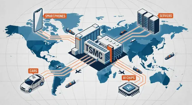
TSMC isn’t a household name, yet it quietly sits behind many of the products and services people rely on every day. If you’ve used a recent smartphone, bought a car with advanced driver-assistance features, streamed video, trained an AI model, or run a business on cloud software, you’ve benefited from chips that were likely manufactured by TSMC.
A strategic bottleneck is a point in a system where capacity is limited, alternatives are scarce, and delays cascade outward. Think of a single bridge on the only road into a city: even if everything else is working, traffic backs up at that one spot.
TSMC is that bridge for advanced chips. Many companies can design chips (Apple, NVIDIA, AMD, Qualcomm, and thousands more). Far fewer can manufacture them at the most advanced “nodes” with high yield, high volume, and consistent quality. When the world wants more cutting-edge chips than the available factory capacity, the constraint isn’t creativity—it’s production slots.
Modern products are basically “systems of chips.” Phones depend on efficient processors and radio chips. Cars increasingly depend on microcontrollers, power chips, sensors, and AI accelerators. Cloud data centers scale only if they can continually deploy new CPUs/GPUs. AI progress is tightly tied to access to the newest, fastest accelerators—because software improvements still need hardware to run.
This is a business-model and supply-chain story, not a deep dive into physics. We’ll focus on who makes what, why manufacturing is hard to replicate, and how concentration created leverage.
Along the way, we’ll answer four practical questions: Why TSMC specifically? Why is this problem more urgent now? Where do the real constraints appear between design and wafers? And what could realistically change—through new fabs, policy (like the CHIPS Act), or shifts in how companies source chips?
A semiconductor foundry is a company that manufactures chips for other companies. Think of it like a high-end factory that can produce millions of identical, extremely precise products—except the products are tiny circuits.
A fabless company designs chips but doesn’t own a factory (“fab”). For example, Apple designs the A-series and M-series chips, and NVIDIA designs GPUs, but they typically hire a foundry to build them.
An IDM (Integrated Device Manufacturer) does both design and manufacturing under one roof. Intel is the classic example: it historically designed many of its CPUs and also manufactured them in its own fabs.
When design and manufacturing separated, chip designers could focus on performance, power efficiency, and features—without spending tens of billions building and upgrading factories. At the same time, foundries could focus on the hardest part: repeatedly producing tiny, defect-free patterns at enormous scale.
This specialization accelerated innovation because more companies could afford to “enter” chip design, and they could iterate faster by tapping the same manufacturing platform.
Running a leading-edge fab is a constant cycle of expensive upgrades, process tuning, and high-volume production. Foundries spread those costs across many customers, so their business model naturally rewards scale and manufacturing focus.
TSMC is the best-known pure-play foundry and the default choice for many advanced chips. Samsung also offers foundry services but balances them with its own chip products. Intel is expanding its foundry ambitions, but its history is primarily IDM—meaning the transition involves both technical and business model changes.
TSMC didn’t become central by accident—it was built around a simple idea that sounded boring at the time: be a factory for everyone, and compete on execution rather than on owning the end product.
TSMC was founded in 1987 with backing from Taiwan’s government and a mission focused on manufacturing. In the 1990s, it won early customers who wanted to design chips without owning expensive factories. That timing mattered: the “fabless” model (companies that design chips but don’t manufacture them) was starting to take off.
By the 2000s, the fabless ecosystem was no longer niche—think smartphone and networking chip designers that needed fast iterations and predictable production. As the 2010s pushed performance and power-efficiency harder, TSMC kept moving to newer process generations ahead of most alternatives, which made it the default choice for the most demanding designs.
TSMC’s edge came from three reinforcing advantages.
First, process leadership: it repeatedly delivered new manufacturing “nodes” that improved performance and efficiency. Second, customer trust: it built a reputation for protecting customers’ intellectual property and for not competing with them by launching its own chips. Third, execution: it scaled complicated production reliably—on schedule, at high yields, and in massive volumes.
That combination is hard to beat. A chip designer can tolerate a slightly higher wafer price; it can’t tolerate late delivery, low yields, or surprise changes in the manufacturing process.
A pure-play foundry manufactures chips for other companies and does not sell its own competing processors. That’s different from integrated device manufacturers (IDMs) that both design and make chips, and it’s also different from foundry businesses inside companies that still have internal product priorities.
For fabless companies, this neutrality is a feature: it reduces conflicts and makes long-term roadmaps easier to share.
A “node” (like 7nm, 5nm, 3nm) is shorthand for a generation of manufacturing technology. Smaller nodes generally allow more transistors in the same area and can improve speed and/or reduce power use—key for phones, data centers, and AI accelerators.
Getting to each new node requires huge R&D spending, specialized tools (including EUV lithography), and years of learning. TSMC kept absorbing that complexity so its customers could focus on design—and that’s how it became the default factory for advanced chips.
Advanced chipmaking isn’t “just building a factory.” It’s closer to running a physics lab that ships millions of identical products—where tiny deviations can ruin an entire batch. That combination of scientific precision and high-volume reliability is what makes leading-edge manufacturing so difficult to copy.
At advanced nodes, features on a chip are so small that dust, vibration, or minor temperature swings can cause defects. That’s why modern fabs rely on extreme clean rooms, tightly controlled airflow, and constant monitoring of chemicals, gases, and water purity.
The hard part isn’t only achieving those conditions once—it’s maintaining them 24/7 while running thousands of process steps. Each step (etching, deposition, cleaning, inspection) must line up with every other step, or the final chip fails.
A leading-edge fab requires an enormous amount of specialized equipment, redundant utilities, and supply infrastructure. The building itself matters, but the real investment is the toolset, the support systems, and the ability to keep them running at high utilization.
This is why “catching up” is rarely a one-time spend. The equipment must be installed, calibrated, integrated into a stable process flow, and then upgraded repeatedly as nodes advance.
For the most advanced chips, EUV lithography is a key enabling technology. EUV tools are among the most complex machines ever commercialized, and only a small number can be produced and delivered each year.
That creates a natural bottleneck: even well-funded new entrants can’t instantly scale without access to these tools and the ecosystem of parts, service, and process know-how that surrounds them.
Even with the same tools, two fabs won’t get the same results. Experience shows up as higher yield (more good chips per wafer), faster ramp times, and fewer production surprises.
That advantage is built from talent, hard-won “yield learning” over many product cycles, and operational discipline—thousands of small decisions that compound into dependable output. This is the quiet reason replication takes years, not months.
It’s easy to think chip “manufacturing” starts when a wafer enters a fab. In reality, the tightest constraints often show up earlier—at the handoff points where decisions become harder to reverse and schedules get locked.
A simplified path looks like this:
The catch: each step feeds requirements back into the previous one. A packaging choice can force design changes; a yield problem can trigger a redesign.
Delays cluster around tape-out readiness, mask availability, and fab queue time. A late design fix can miss a reserved slot; missing a slot can mean waiting weeks or months for the next window. That pushes packaging and test schedules, which then delays shipping and product launches.
Another common bottleneck is packaging capacity, especially for high-end chips that need complex interconnects. Even if wafers are finished, a packaging backlog can stall delivery.
Foundry capacity is largely allocated through reservations made well in advance. Customers forecast volumes, pay for commitments, and plan tape-outs to match available slots. When demand shifts suddenly, reshuffling isn’t instant—tools and processes are tuned for specific nodes and products.
Yield is the share of usable chips per wafer. Small yield drops can dramatically reduce output and raise effective cost. For advanced nodes, getting yield up is often the difference between “we can ship” and “we’re constrained,” even when the fab is running at full speed.
TSMC’s order book looks diversified on paper, but the most advanced capacity (the “leading edge”) tends to attract the same kinds of products at the same time. That’s not an accident—it’s a consequence of physics, economics, and product cycles.
High-end smartphone processors, data-center CPUs/GPUs, and many AI accelerators all chase the same benefits: more performance per watt and more compute per square millimeter. The newest nodes (enabled by tools like EUV lithography) are where those gains are most available.
Because leading-edge fabs cost tens of billions to build and equip, only a few sites can run at that frontier—and designers want the best process the moment it’s ready. The result is clustering: multiple “must-win” products landing on the same small pool of capacity.
TSMC simultaneously serves:
In normal times, that mix is efficient. A single foundry can smooth out seasonal swings (holiday phone launches vs. enterprise refreshes), keep equipment utilized, and standardize around proven design tools and packaging options.
Concentration becomes painful when demand spikes or a major customer shifts strategy. A surprise smartphone rebound, a sudden AI boom, or a big GPU launch can soak up wafers that other customers assumed would be available. And when one customer pulls demand forward (ordering earlier “just in case”), others often follow—amplifying shortages.
Even if factories run 24/7, leading-edge capacity can’t be expanded quickly. The practical effect is that product roadmaps—across phones, cloud, and AI—start competing for the same limited slot on the calendar.
A “choke point” isn’t only about one factory being busy. It’s about many critical paths narrowing into a few places that are hard to substitute quickly. With advanced chips, TSMC sits near the center of several single points of failure at once.
Even if you have multiple chip designers, you may still depend on the same small set of things:
A disruption in any one of these can delay output—then the delay ripples to everything downstream.
Recent years showed how fast “normal” assumptions can break:
Just-in-time practices cut costs, but they also remove slack. When lead times stretch from weeks to months, “efficient” inventory levels turn into missed launches, production stoppages, and expensive spot buying.
Non-technical risk planning often boils down to a few levers: dual-source where feasible, hold targeted buffers for long-lead parts, and redesign products so they can accept alternate nodes or substitute components. The goal isn’t to eliminate dependence—it’s to avoid one surprise becoming a company-wide shutdown.
TSMC sits at an unusual intersection: it’s a private company, but it produces advanced-node chips that power phones, cloud services, AI accelerators, and critical industrial systems. When so much of the world’s leading-edge capacity is concentrated in one place, location stops being a footnote and becomes a policy concern.
Taiwan’s position—both geographic and political—creates a dependency that many governments and large buyers can’t ignore. Even without any dramatic event, cross-strait tensions raise questions about continuity: shipping lanes, air freight, insurance, and the ability to move people and parts quickly. The “global supply chain” risk here isn’t abstract; it’s about whether wafers, chemicals, and finished chips can keep flowing on schedule.
Advanced chip manufacturing is tightly coupled to a small set of specialized inputs: EUV lithography systems, process chemicals, and design software. Export controls can restrict any of these—equipment shipments, spare parts, service visits, or even which customers can receive certain chips.
That matters because the semiconductor foundry model connects many countries at once: fabless companies may design in one place, use tools from another, and fabricate through contract chip manufacturing somewhere else. When rules change, it can create bottlenecks even if factories stay physically intact.
Policies like the CHIPS Act aim to increase resilience through domestic capacity and “strategic autonomy.” But building new fabs takes years, experienced talent, and long-term demand. The incentives are strong; the constraints are real—so progress tends to be gradual rather than instant.
Yes—but “diversify” is a long, uneven journey rather than a switch you flip.
Building fabs in more regions (the U.S., Japan, and Europe under programs like the CHIPS Act) can reduce single-location risk and improve resilience in the global supply chain. It also helps with proximity to customers in autos, cloud, and defense. But it doesn’t automatically recreate the specific advantages that make TSMC the default for advanced-node chips.
A fab is only the visible part. The harder part is the surrounding ecosystem: materials, specialty chemicals, wafer suppliers, packaging, testing, and the dense network of fabless companies and engineers who know how to ramp yields at scale. Even if a new facility has the same “nameplate capacity,” it may take years to match real output of high-yield, high-performance silicon.
Some bottlenecks can’t be accelerated much by money alone:
These constraints make “contract chip manufacturing” capacity less like a commodity and more like a craft learned over cycles.
Diversifying foundry footprint often means choosing between cost (new builds are expensive), speed (ramps are slow), ecosystem depth (supplier density varies), and operational maturity (yield learning curves). A region can improve on one dimension while lagging on another.
Watch four signals:
Diversification is happening—but the gap between “a fab exists” and “it reliably produces cutting-edge chips at scale” is where TSMC’s advantage persists.
People often talk about “advanced chips” as if the whole industry is one race to the smallest nanometer number. In reality, there are two supply problems that behave very differently: leading-edge nodes (the newest, smallest transistors) and mature nodes (older, widely used processes).
Leading-edge chips—think the processors in flagship phones, data-center accelerators, and high-end PCs—depend on the newest tools, the tightest process control, and a small set of fabs that can run them at high yield. Capacity is scarce because building it is expensive and demand is volatile: a single product cycle or AI wave can swing orders dramatically.
A lot of the most painful disruptions in recent years weren’t about the latest smartphone chip. They were about mature-node components used everywhere: power management ICs, display drivers, microcontrollers, connectivity chips, and sensor interfaces. Cars and appliances need huge volumes of these parts, and qualification cycles are long—automakers can’t just swap in a “close enough” replacement without re-testing and re-certifying.
Foundries tend to add leading-edge capacity when they see high-margin, high-commitment demand (often from a handful of large customers). Mature-node expansion is a different bet: margins are thinner, but demand is steadier—until it isn’t. When mature-node demand spikes, adding capacity can take longer than expected because the business case is less straightforward.
Even when wafers are available, chips still need to be packaged and tested. Advanced packaging (like chiplets, 2.5D/3D stacking, and high-bandwidth memory integration) can become its own bottleneck, with limited equipment, materials, and specialized know-how. That means “more wafers” doesn’t automatically translate into “more shippable chips.”
No company can “opt out” of the foundry ecosystem overnight, but tech teams can reduce how often one factory decision determines their product roadmap.
Multi-sourcing isn’t just approving two suppliers on a slide. It usually means qualifying a second process node and a second package/test path.
A practical approach is to split risk by tier: keep a leading-edge version for flagship products, and maintain a second implementation on a more available node for mainstream SKUs. That second version won’t match peak performance, but it can protect revenue when allocation gets tight.
Design teams can “pre-bake” fallback options: libraries, IP blocks, and package choices that can be moved with fewer surprises. Even small choices—voltage margins, SRAM density assumptions, or a packaging dependency—can lock you into one foundry flow.
This is where design-for-manufacturability matters: co-develop with the foundry and OSAT early so the design tolerates process variation, has realistic yield targets, and avoids exotic steps that only one site can run.
Inventory is expensive, but targeted buffers for long-lead components (substrates, power management ICs, microcontrollers) can prevent “one missing part” from stopping shipments.
Long-term capacity agreements (LCAs) change behavior: engineering prioritizes stable nodes, product teams freeze specs earlier, and procurement gains clearer allocation rights. The tradeoff is less flexibility—so negotiate change clauses up front.
Ask for specifics, not reassurance: typical and worst-case lead time, allocation rules during shortages, whether priority is tied to prepayments/LCAs, where wafers are fabbed and packaged, and what qualifies as an “approved” alternate. These answers determine your true dependency profile.
One of the most practical ways to reduce “surprise” dependency is to make it measurable: a lightweight internal dashboard that maps each product to its node, foundry, package/test path, critical materials, and lead-time assumptions. That kind of visibility often turns vague supply-chain risk into concrete engineering and procurement work.
If you’re building these internal apps, a vibe-coding platform like Koder.ai can help teams prototype and ship the software quickly—using a chat interface to generate a React web dashboard with a Go + PostgreSQL backend, then iterating in a planning mode before committing changes. The key is speed: the faster you can model constraints and test scenarios, the less you rely on heroic coordination when capacity tightens.
If you don’t follow semiconductors for a living, the easiest mistake is to treat chip supply as a yes/no question: either there’s a shortage or there isn’t. In reality, the early warning signs show up months (sometimes years) before prices move or products slip.
Capex cycles (factory spending): When TSMC and peers raise long-term spending plans, it suggests confidence in demand—but it also signals when new capacity might arrive. Watch not just the headline number, but whether spending is shifting to leading-edge fabs, mature nodes, or packaging.
Tool delivery backlogs: Advanced tools (especially EUV) are built in limited quantities. If tool makers talk about multi-year backlogs, that’s a quiet way of saying capacity expansion will be slow, even with money on the table.
Packaging capacity: More performance now depends on advanced packaging. If packaging lines are constrained, “enough wafers” still won’t translate into enough shippable chips.
Companies use careful wording:
If an announcement skips directly to “volume,” look for evidence: customer names, shipping timelines, and whether packaging is included.
For more explainers and updates, browse /blog.
A strategic bottleneck is a constrained point where capacity is limited, alternatives are scarce, and delays cascade through the rest of the system. For advanced chips, the bottleneck is often not chip design talent—it’s the limited number of factories that can reliably produce leading-edge wafers at high yield and high volume.
TSMC’s leverage comes from consistently combining:
Many firms can design great chips; far fewer can manufacture them at the frontier on schedule.
A foundry manufactures chips for other companies.
The split lets designers iterate faster without building fabs, while foundries win by specializing and scaling manufacturing.
A “node” (e.g., 7nm, 5nm, 3nm) is shorthand for a generation of manufacturing technology. Newer nodes generally improve performance per watt and/or transistor density.
In practice, choosing a node is also choosing:
Advanced manufacturing is hard to replicate because success requires more than money and buildings:
Two fabs with similar equipment can still produce very different yields and reliability, which determines real output.
EUV (extreme ultraviolet) lithography is a critical tool for patterning the smallest features in leading-edge chips. It matters because:
So even well-funded expansion can be gated by tool supply and integration timelines.
Common constraints appear at handoff points where schedules become hard to change:
A slip early can push packaging, test, and shipping—turning a weeks-long issue into a quarter-long delay.
Yield is the percentage of good, usable chips produced from a wafer. It directly affects:
Small yield changes at advanced nodes can translate into big supply swings.
Because “more wafers” doesn’t equal “more shippable chips.” After wafer fabrication, chips must be:
Advanced packaging has its own capacity, materials, and equipment constraints, so it can become a separate choke point even when wafer output is strong.
Diversification is happening, but it’s gradual. New fabs can reduce single-location risk, yet the hardest parts take time:
To evaluate progress, focus on shipped volume, proven node capability, ramp/yield performance, and whether flagship designs actually migrate.